| Back to Index |
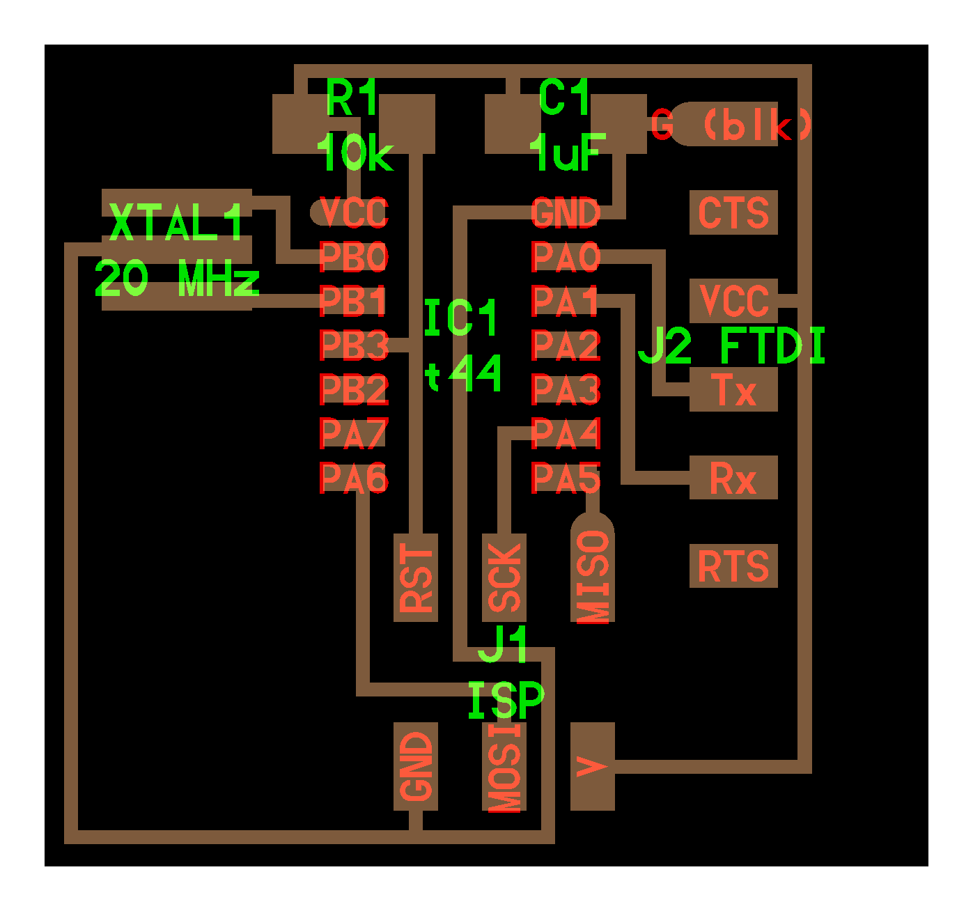
I used Eagle to lay out my schematic and circuits. It's ... not the best. I may try KiCad for my next circuit layout. The tutorial session with Joe Negri, while two hours long, was very helpful, especially in figuring out how to search for the right components in the library: use asterisks on either side of your search term (e.g. *item*)! Even knowing which search terms to use wasn't easy (try the abbreviations used on the board layout, seen below), and knowing which component to use wasn't either. Generally, the item with the word "FAB" on the end was the one to go with. Also, I deleted all the pre-installed Eagle libraries, so I wouldn't have to scroll past tall of them to get to the fab library.
Being meticulous and methodical is key to not driving yourself crazy! Diligently check all the lables to make sure you're connectig the right things to the right things. The major issue I ran into while working with Eagle was that the netting (the lines connecting component to component on the schematic) appeared to be successfully connected, the bright green line turning to dark green, but the corresponding yellow line on my board, indicating which components should connect to each other, was conspiculously absent. When I zoomed waaaaaay in on my schematic, the netting overlapped the pins it was connecting to by a good margin. I deleted the netting, and reconnected it so only a dark green circle appeared in the overlap. This fixed the issue.
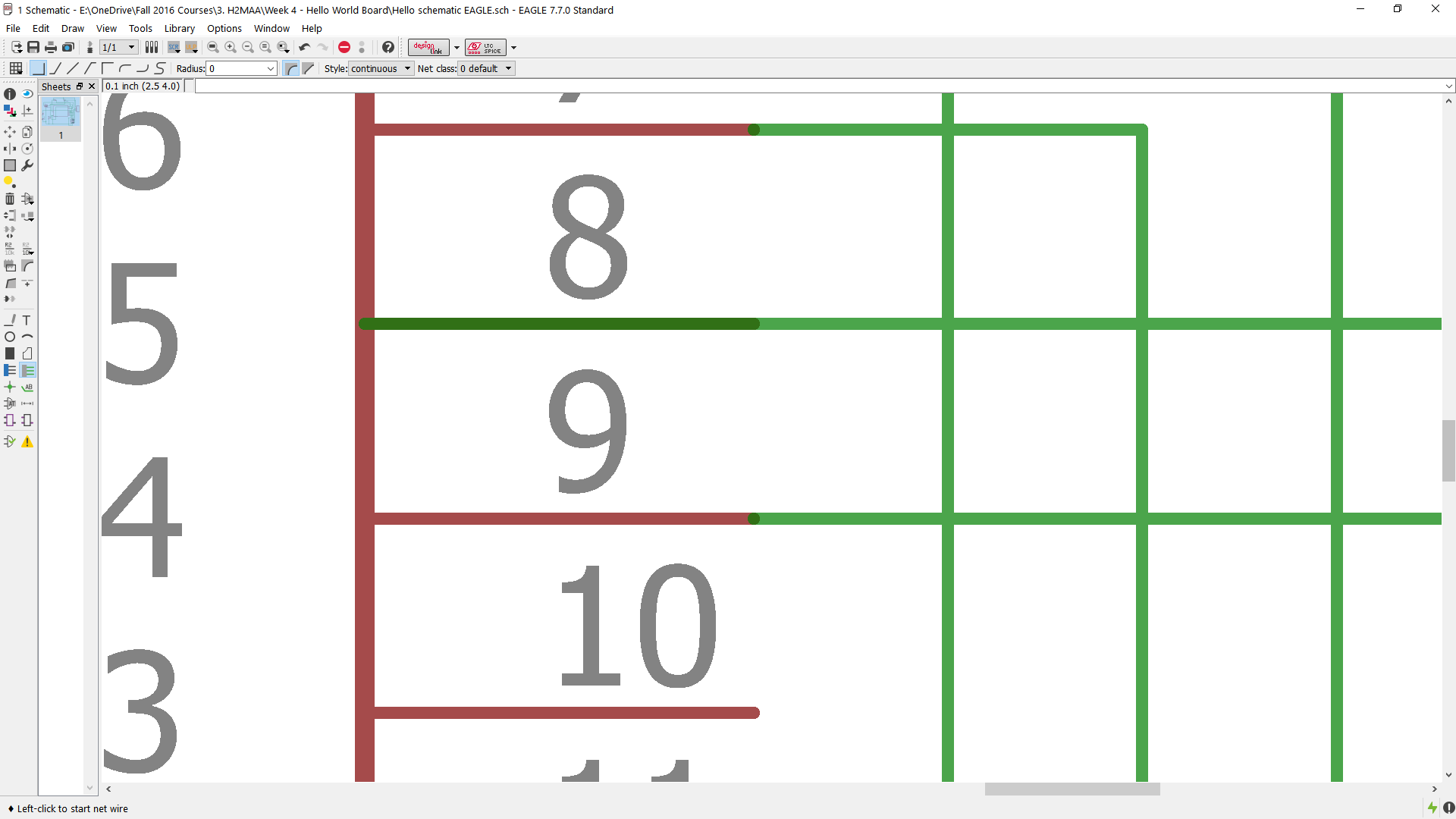
(Dark green overlap on #8: bad. Tiny green overlap on #9: good.)
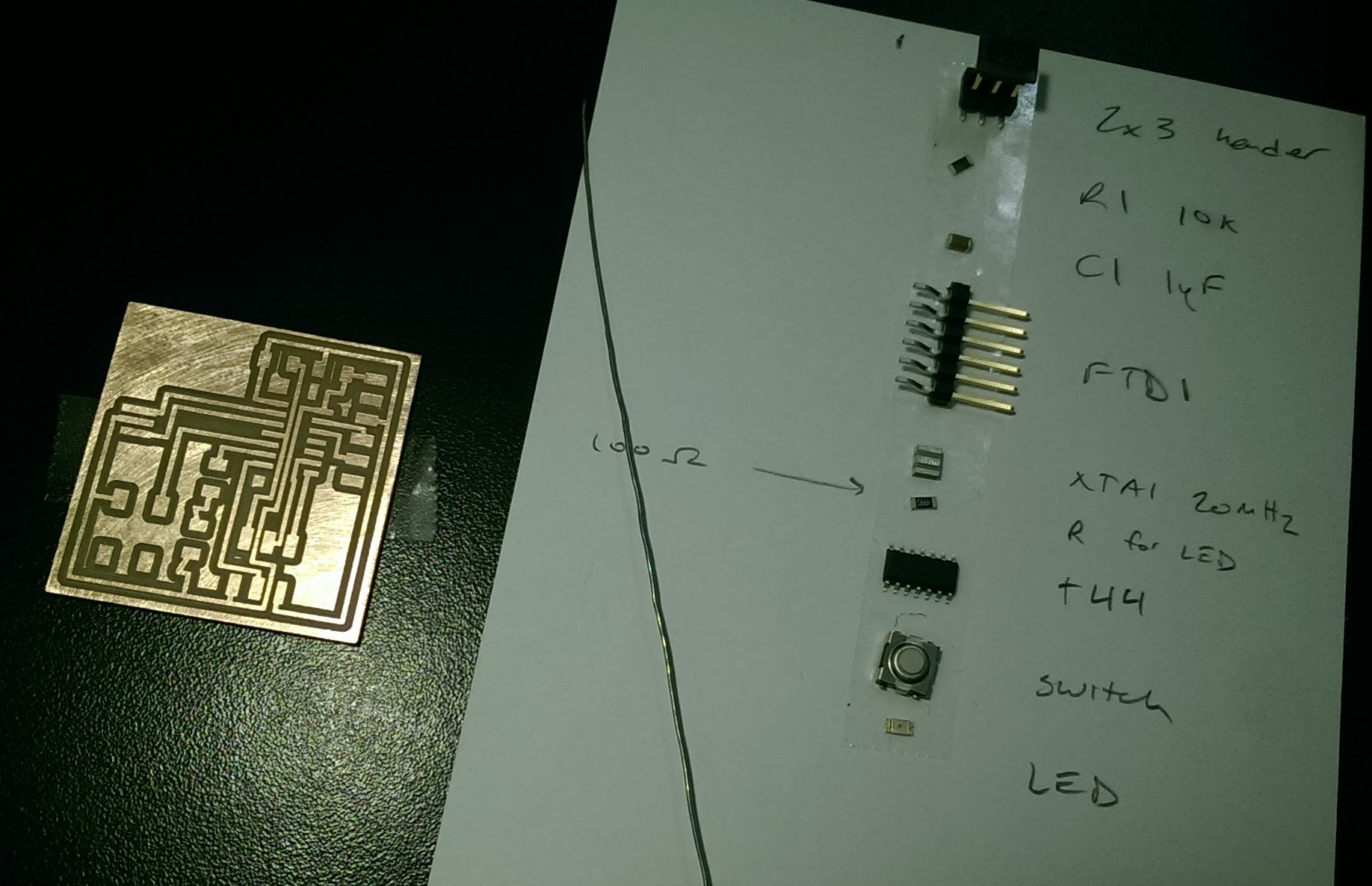
Drawing the traces was kind of fun, actually. Changing the 'alt' settings under Grid to the smallest possible helped improve fine control over the trace layout. I'm not brave enough to attempt a radically different board layout, so I was happy just replicating the prexisting one. Plugging in a button (a "switch"), an LED, and a resistor wasn't too scary.
Board layout completed, I ran into a couple issues between exporting my board from Eagle and the actual physical process of milling them out. I exported my board (top layer only) as an image (png), in monochrome, at 1500 dpi. When I opened the png to edit it, I discovered tiny bumps had been added to the edges of many of my traces. Not sure why.
When I plugged that png into the fab module to calculate the milling path, the result seemed unaffected. So, an inconsequential error, but annoying. I opened the png in Paint to crop to my board size and add an outline. While I was in there, I cleaned up the bumps to soothe my OCD.
I saved my cropped-and-outlined board from Paint, and uploaded those pngs to the fab module, to check the milling path. Two more issues popped up.
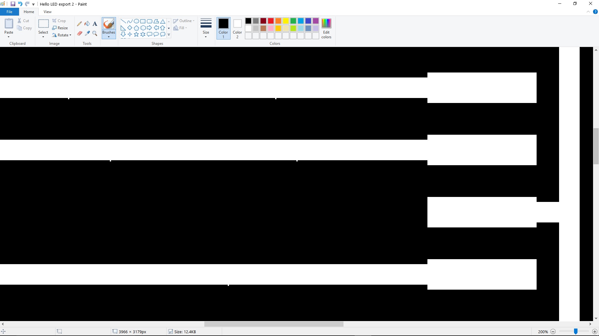
1. In making my outline, I drew a white box around my traces, filled the traces in with black, and saved the resulting outline. When I calculated its milling path, two bizzarre circles showed up in the middle of my board. I went back to the png, and sure enough, there were two stray white pixels that didn't get painted black with the rest of the traces. An easy fix, and a reminder to always check the tool path!
(See those two white dots in the black field on the left? Yeah, I didn't either.)
2. After editing my board in Paint, I saved the pngs and plugged them in to the module. The routing path left something to be desired.
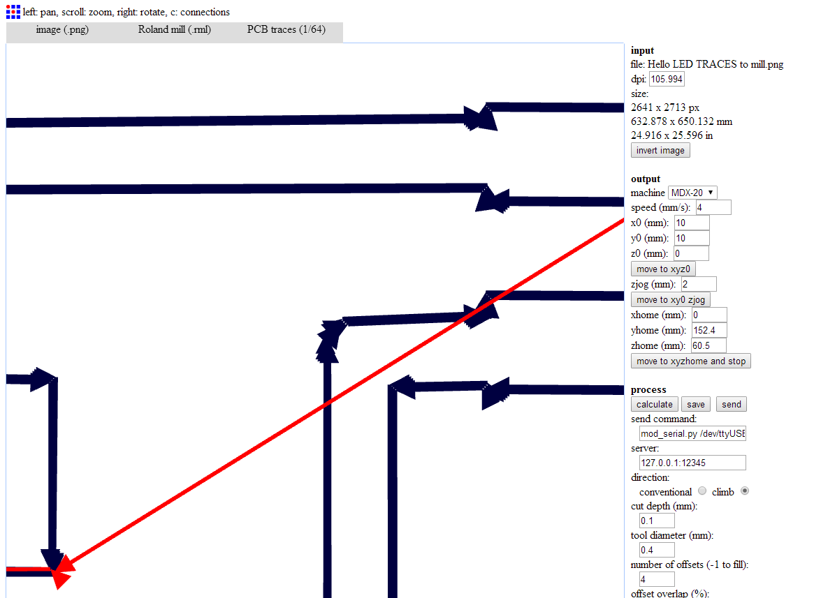
When I checked the routing path using the direct-from-Eagle png, all was well. I hadn't touched the module settings between calculating for that image and calculating from my edited images, but a closer examination revealed that the dpi for my edited images was waaaaaay down at 105, rather than the Eagle-exported 1500. I changed the dpi on the fab module, and the routing path looked much more reasonable.
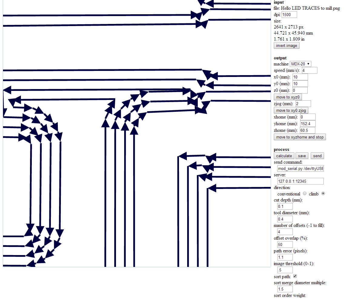
However, it was pointed out to me that the scale might be wrong. When I had cropped my board in Paint, I did it by dragging and selecting the board size, cutting that image out, and pasting it in a new Paint file. This evidently reset the DPI to Paints default, 105-ish. By doing all my editing in the original 1500 dpi file, I was able to create my traces and outline pngs while maintaining the proper dpi. Rechecking these new pngs in the Module results in a good milling path.
HOWEVER. When I reopened those same pngs in Paint, it had automatically changed the dpi to 105. So, I could open a 1500 dpi png in Paint, edit and save it as 1500 dpi, but once that window was closed, I could not reopen it in Paint without messing up the dpi. It's a one-and-done sort of deal. That'll be annoying with more complex boards which I may have to go back and edit, so I'll need to learn a new program (Inkscape, GIMP, Photoshop, etc.) for future trace editing needs.
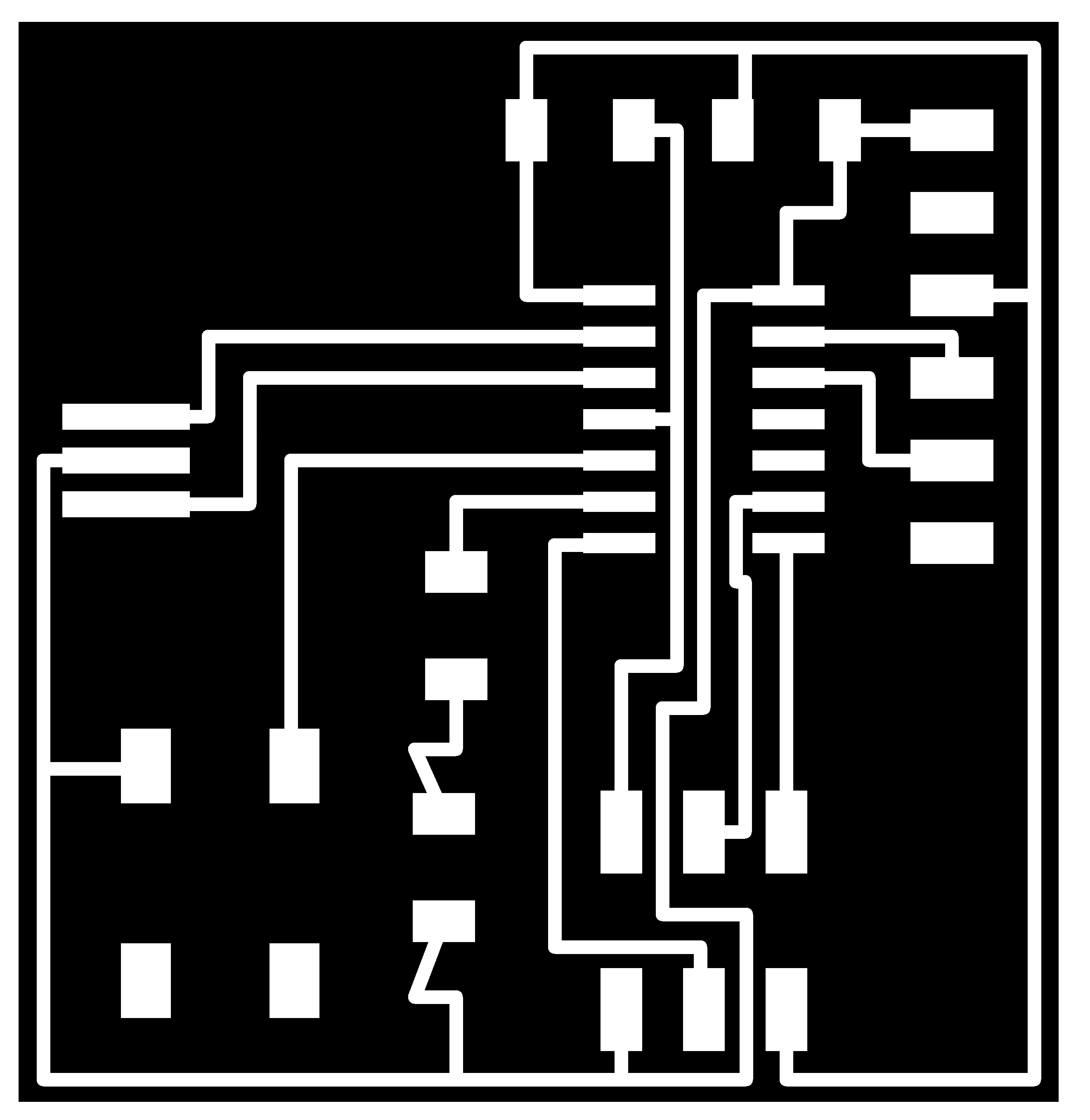
After milling out my first take at the circuit design, two issues became apparent. First, my outline was too close to my traces, and the border of the board was also a trace. No bueno. Second, even though the spacing on the board design looked totally fine, the routing path, in fact, was not. Three traces weren't separated from the pads they ran close to.
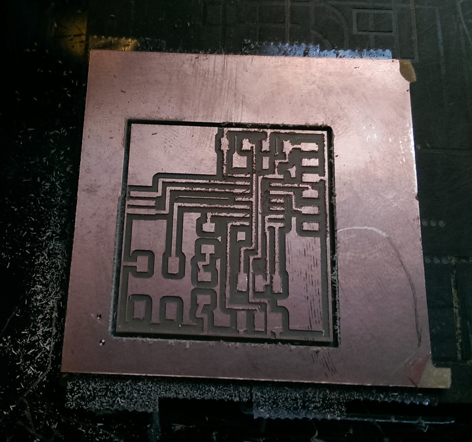
(See lowest-right pad on the board, lowest of the ATTiny pads, and lowest of the resonator pads on the left.)
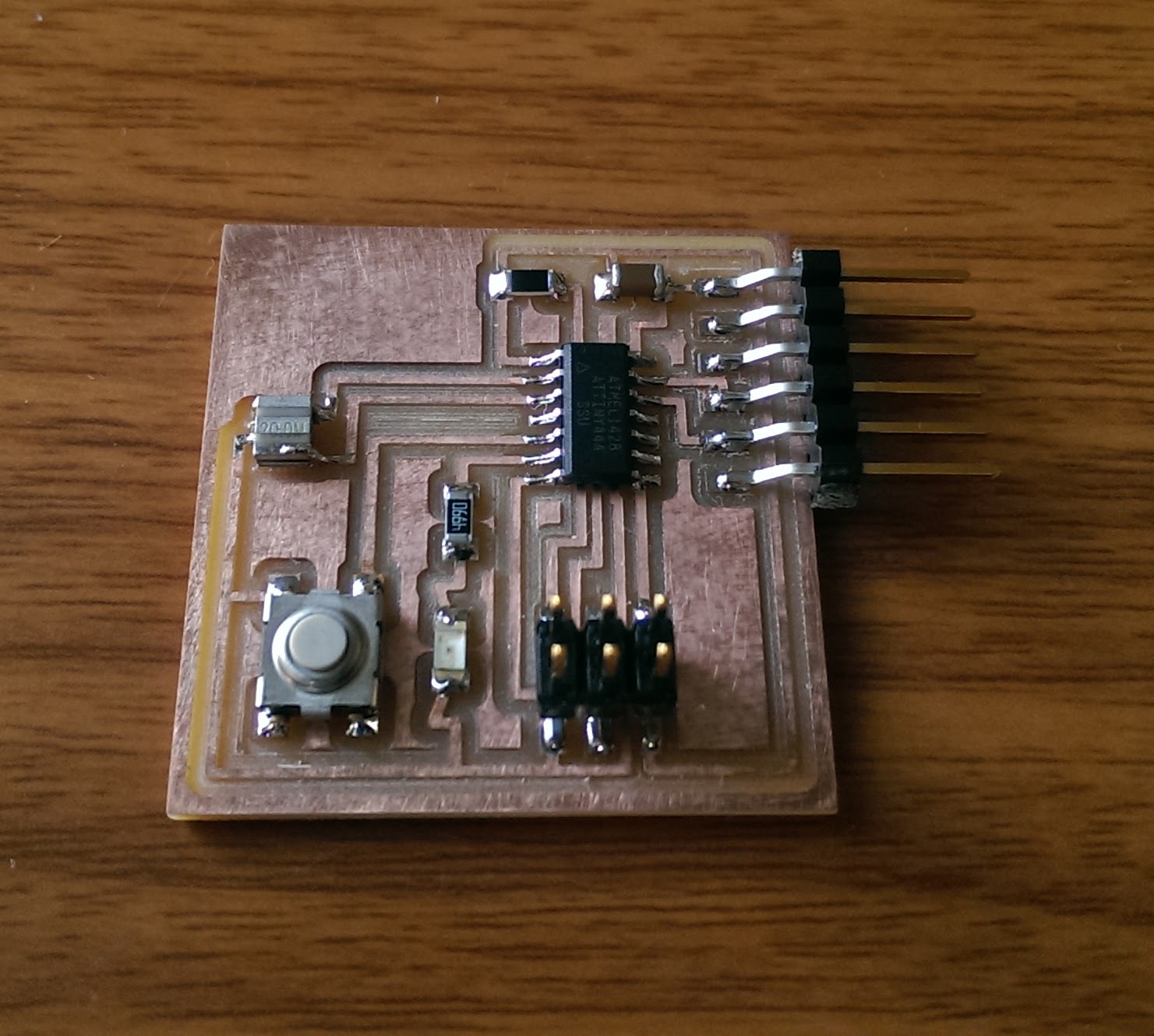
After some quick editing (in paint, because that's what was on the shop computer), my second board came out much better. Solder, stuff, plug it in!